
Growth of bulk β-Ga2O3 crystals from melt without precious-metal crucible by pulling from a cold container
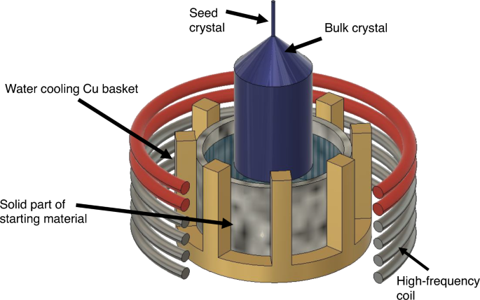
During our experiments with the Ga2O3 melting in a cold container, it was found that varying the generator power mainly leads to changes in the melt volume, resulting in only minor changes in the temperature of the melt surface. Moreover, after decreasing the generator power to a certain value, the volume of melt decreased markedly, and due to the power distribution to the remaining melt, its temperature increased further. In the case of the 5 MHz vacuum tube generator (such generators are usually manufactured according to a self-excited circuit), the generator power was the only parameter possible to control. For diameter control, we used a similar method to the one applied before for the growth of Gd-Al-Ga garnet—air flow through a ceramic pipe over the melt surface using a cooling fan placed outside the growth chamber. By varying the speed of the cooling fan, it was possible to change the melt surface temperature and control the growing crystal diameter.
In the experiments with a larger Cu basket and lower frequency SiC generator, we varied the generator frequency across a wide range, in addition to varying the power. This method was found to be more effective for controlling the diameter. The frequency range for the control was 430–470 kHz with constant power generation. During the growth process, periodical fluctuations were observed in the melt temperature similar to that observed in the traditional cold crucible technique. The stabilization of such phenomena was realized by automatic frequency adjustment to maintain a constant phase difference between the voltage and current of high frequency power.
Phase difference control (frequency control) of the oscillator was introduced to observe the progress of melt solidification in the cold container and to stabilize the temperature gradient in the melt by stabilizing the amount of heat generated by the object being heated. In the series resonance circuit shown in Fig. 3a, the phase difference θ is as follows.
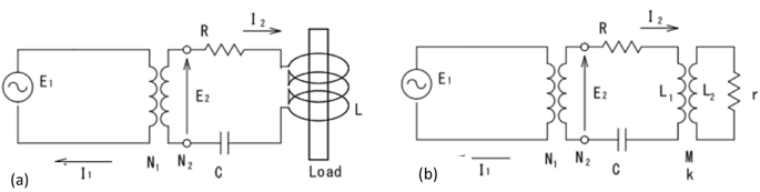
Series resonance circuit (a) and circuit with heating object (b).
$$\theta ={tan}^{-1}{\left(\frac{2\pi fL-\frac{1}{2\pi fC}}{R}\right)}^{2},P=VIcos\theta$$
The equivalent circuit in this figure is shown in Fig. 3b, where r is the resistance of the object to be heated (oxide melt). The resistance R of the circuit is coupled to the object to be heated through the work coil, and when r changes, R also changes according to the coupling coefficient k and mutual inductance M. Therefore, when the volume of the melt changes due to solidification, the resistance of the circuit changes, which can be observed as a phase difference, and controlling the oscillation frequency to keep the phase difference constant prevents a decrease in heat generation and stabilizes the melt state.
In practical experiments, the measurement and comparison of phase signal were made using a digital power analyzer (Pos 16 on Fig. 2). The graphical meaning of phase difference and real image in the oscilloscope at the completely melted Ga2O3 conditions are shown in Fig. 4. Phase difference close to zero is the most efficient operating mode of the generator. However, to prevent the destruction of SiC transistors in the case of operation at the exact resonance conditions, the automatic system was maintained such that the difference between the magnitudes of the generator and resonance frequencies was at least 1000 Hz.
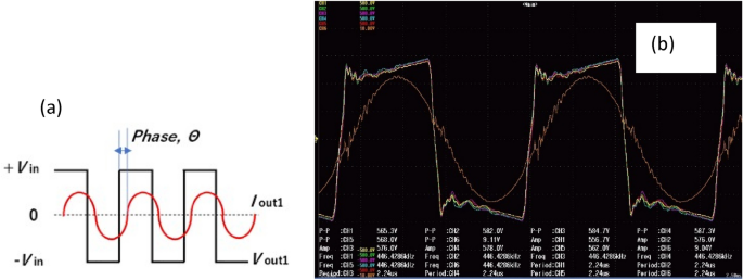
The meaning of phase difference and the real oscilloscope image. Ch. 1–5–output voltage signals of five SiC power modules, Ch. 6 (orange line)–current signal of one SiC module.
After the final melting of raw materials, the frequency shift needed for retaining the same phase difference as before the melting was ~ 10–15 kHz. These values were observed with the use of a 4-turn RF coil with a coil height of 50 mm. Our previous experiments on melting Gd-Al-Ga garnet in the same size Cu basket demonstrated that the frequency change after the final melting of the raw materials was ≤ 2–3 kHz19. These data are in good agreement with the higher electric conductivity of undoped Ga2O3 melt. When crystal expansion initiates, the phase difference (and respective melt temperature) gradually increased with increasing generator frequency using the control software.
Figure 5 illustrates key steps during the OCCC method processing, from seed touching to the growth of bulk β-Ga2O3 crystals.
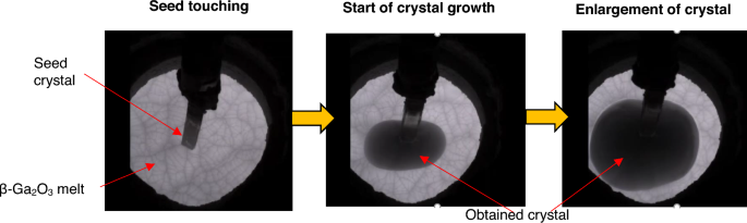
Stages in the OCCC method procedure. From left to right: seed touching, initial crystal growth, and enlargement of the bulk β-Ga2O3 crystal.
Figure 6 shows the internal view of the copper basket after the β-Ga2O3 bulk crystal growth using the OCCC method is complete. The thin white area lining the copper basket pipes is unmelted sintered Ga2O3, and an area around the center of the basket contains several transparent crystal blocks that have melted and solidified.
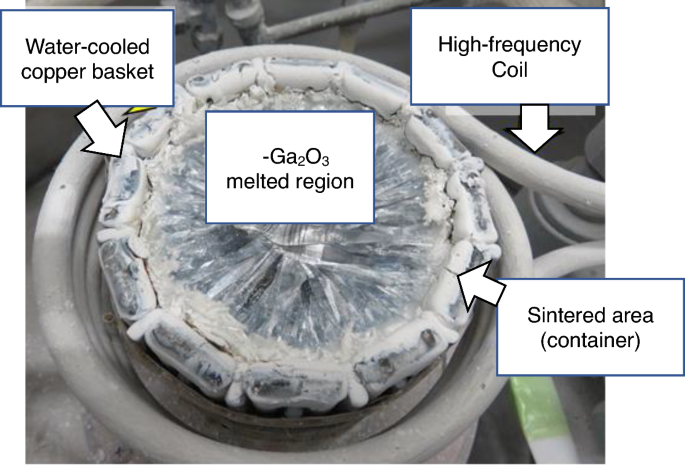
Top view of the copper basket after cooling during β-Ga2O3 bulk crystal growth via the OCCC method.
Crystals grown using a 60 mm Cu-basket and the 5 MHz generator are shown in Fig. 7. For small (10–15 mm) crystal diameters, the interface shape was slightly convex and diameter control was rather easy. However, upon reaching crystal diameters ~ 20–25 mm, the interface shape became concave and the difficulties in diameter control increased. Often, rapid radial growth to one side of the spiral shape was observed (Fig. 7c). Figure 7b shows the biggest crystal grown using the 60 mm basket and 5 MHz high frequency, which measured 30 mm in diameter and 30 mm in length. Larger diameter crystals were grown using 85- and 100-mm diameter baskets with 430–470 kHz power supply with frequency control.
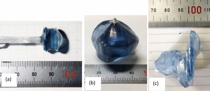
Photographs of β-Ga2O3 single crystals grown using a 5 MHz generator. (a) β-Ga2O3 single crystal with seed crystal. The size is ~ 10 mm in diameter and ~ 10 mm in body length. (b) β-Ga2O3 single crystal. The size is ~ 1 inch in diameter and ~ 15 mm in body length. (c) β-Ga2O3 single crystal with spiral growth.
In our initial experiments, the seed crystals frequently melted during seeding due to unoptimized temperature distribution on the surface of the melt. Careful selection of the operation frequency range along with optimization of the shape of the ceramic hot zone were required for successful seeding. Under the conditions used in the present study, β-Ga2O3 single crystals with diameter ≤ 46 mm were grown successfully (Fig. 8). All grown crystals were transparent and slightly bluish in color. The solid–liquid interface shape during the growth of β-Ga2O3 single crystals was strongly dependent on the liquid layer thickness in the 85 mm Cu basket. In the case of relatively short layer thickness (10–15 mm), the interface shape was concave, and stronger melt temperature periodical fluctuations were observed. However, in the melt layer ≥ 20–30 mm, the interface shape was slightly convex and growth was more stable. Melt height within certain limits could be controlled by ignition conditions and the shape of the RF coil. Furthermore, the interface shape may also be controlled via a careful selection of the crystal rotation rate as in conventional CZ growth. The relatively rapid and sharp expansion of the growing crystal observed in several experiments was caused by the steep temperature gradient. In the case of 85–100 mm Cu baskets and lower frequency SiC generator, we also performed the experiments with cold-air flow to the bottom area of the seed holder. This was sufficient to increase the axial gradient and make rapid crystal expansion more controllable. However, it generated rather strong noise to the crystal weight signal (i.e. noise to signal ratio was high) and created additional difficulties for the crystal shape control.
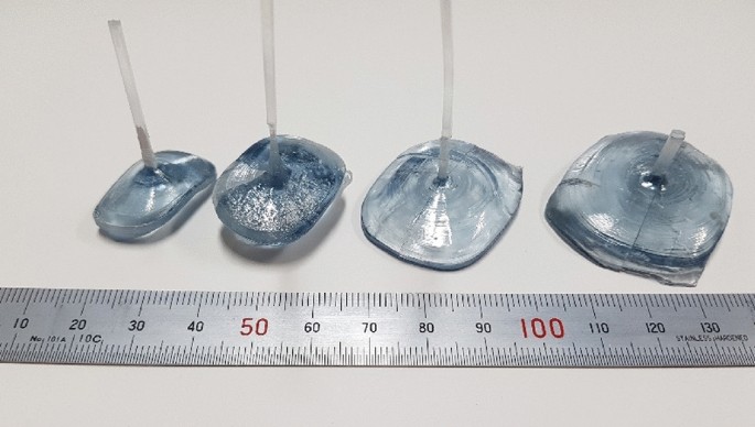
Photograph of β-Ga2O3 single crystals grown in air using the 430–470 kHz SiC generator.
Table 1 presents the results of an impurity evaluation based on GDMS analysis. Si and Fe impurities were observed, whereas the amounts of the materials in the immediate environment of the melt, such as Cu (from the basket) and Zr (from the insulator), were below the detection limit. Si contamination (> 1 ppm), which can be assumed to originate from the raw materials. Fe and other contaminants were believed to have originated from the preparation stage (pressing). The levels of other elements, such as Na, Ti, Mn and Co, Pt, and Ir, were below the detection limit. Pt and Ir were not detected because we did not use a precious-metal crucible; this is a significant difference from the conventional method that uses a precious-metal crucible and impurities of such metals easily can be identified in the grown crystal or solidified melt.
Figure 9 shows a cut and polished sample of the grown β-Ga2O3 crystal and the results of the XRC measurement. A full width at half maximum (FWHM) value of 42 arcsec was obtained. A this FWHM value is comparable than that of β-Ga2O3 grown using the edge-defined film-fed growth method27. At present early stage of OCCC method investigation, it is noticeably lower than those of CZ-grown crystals28. At the start of crystallization, the grain boundaries were observed mainly at the central part close to the seed. For crystals grown with the convex solid–liquid interface shape, the control of the shape was easier and it was possible to expand the crystal to the desirable diameter without excessively rapid radial growth, which often caused the formation of grain boundaries.
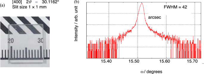
XRC analysis. (a) β-Ga2O3 single crystalline plate used for XRC measurement and (b) XRC pattern of the β-Ga2O3 single crystal grown using the OCCC method.